Product Benefits
The main functions of the IC substrate board include chip soldering and electrical connection by wire bonding or flip chip process, and it guarantees reliability by using adapted raw material for chip elongation.
Reliability
Substrate Like PCB (SLP) is based upon BT (Bismaleimide Triazine) resin material instead of FR4. The BT material has a very high Tg. 250 to 300°C and a very low X&Y CTE 2-5 ppm/°C instead of 11-14 ppm/°C for FR4. This ensures very reliable integration with the IC substrates and creates the possibility to create Modules or Systems in Packages (SIP) with chips or components with high-density design.
Performance
SLP technology uses high-performance materials, the process of the IC Substrate and the stack-ups with laser defined vias known from HDI technology to create a very reliable and ultra complex HDI PCB.
High Density
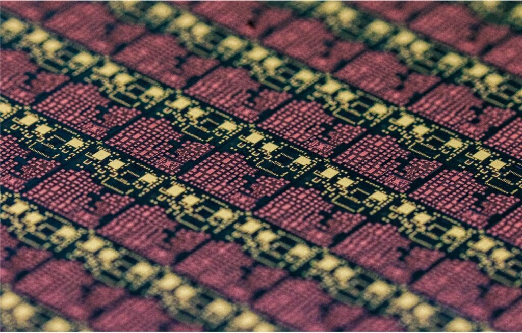
Substrate Like PCB (SLP) brings HDI PCB production to a new level with ultra-fine line/space down to 30/30µm. Common roadmaps of the SLP Manufactories expect to reach line/space 20/20µm in 2024 and 10/10 in 2025.
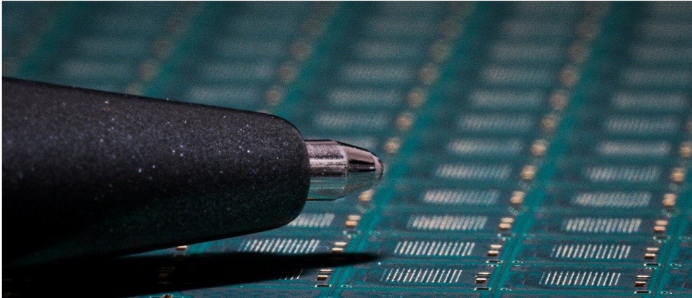
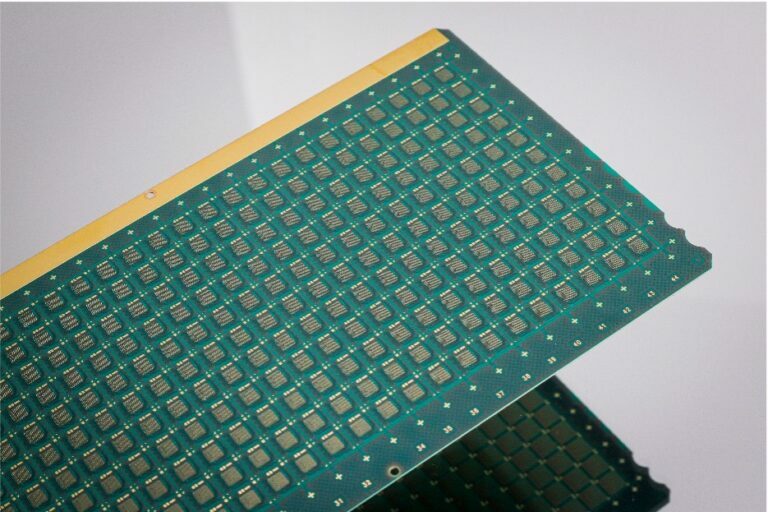
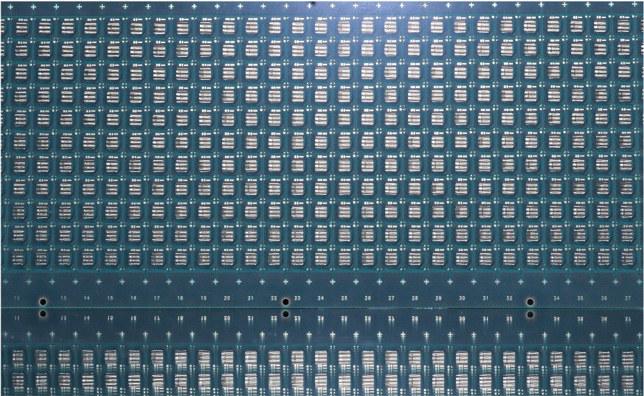
An IC substrate-like PCB (SLP), also known as an IC carrier board, is a type of printed circuit board that is specifically designed to hold integrated circuit (IC) chips. It is an ultra HDI PCB used in the semiconductor industry to package and connect IC chips to the rest of the electronic system.
The main function of an IC substrate PCB is to provide a physical platform for mounting and interconnecting the IC chips. The SLP typically has 2-6 layers of conductive traces, laser-defined vias, and pads that allow for electrical connections between both the IC chips and the PCB.
The main function of an IC substrate PCB is to provide a physical platform for mounting and interconnecting the IC chips. The SLP typically has 2-6 layers of conductive traces, laser-defined vias, and pads that allow for electrical connections between both the IC chips and the PCB.
Line and space: 30/30µm (advanced 20/20µm)
Vias: 50µm Laser defined.
Layer count: 2 to 6, advanced – 6+
Material and others: BT resin, Bismaleimide Triazine
Vias: 50µm Laser defined.
Layer count: 2 to 6, advanced – 6+
Material and others: BT resin, Bismaleimide Triazine
There are 3 different process methods.
Tenting – A subtractive process using thin start Cu foil of 9-12µm and production steps using panel plating. 35/35µm Line & Space possible.
mSAP – A modified semi-additive process using ultra-thin start Cu foil of 1,5µm and production steps using chemical Cu plating + pattern plating process and flash etching. 20/20µm Line & Space possible.
SAP – Semi-additive process using special material without base Cu. and production steps using chemical Cu plating + pattern plating process and flash etching. 15/15µm Line & Space possible. (The SAP method can create up to 12 layers, but it is only available for mass production.)
Stack-up like HDI PCB with core and PP
BT (Bismaleimide Triazine) resin material instead of FR4
BT it’s higher Tg. 250 to 300°C
BT it’s lower CTE XY axis 2-5ppm/°C instead of 11-14ppm/°C for FR4.
Limited to stack-up 2L, 4L, and 6L for standard and 1+2+1, 1+4+1, 2+2+2 for structure.
BT (Bismaleimide Triazine) resin material instead of FR4
BT it’s higher Tg. 250 to 300°C
BT it’s lower CTE XY axis 2-5ppm/°C instead of 11-14ppm/°C for FR4.
Limited to stack-up 2L, 4L, and 6L for standard and 1+2+1, 1+4+1, 2+2+2 for structure.
Double-sided and multilayer PCBs are commonly used in a wide range of electronic applications such as telecommunications, industrial control systems, and power supplies. They are also used in prototyping and small-scale production runs.
Industries
Industries
Telecom
Our desire to stay connected, always and everywhere, is the backbone of ICPRUS’s engineering know-how and one-stop solutions.
Aerospace
ICPRUS is growing in the aerospace industry because of the benefits offered by our expert services and one-stop solutions.
Consumer &
Multimedia
Multimedia
The Industrial Automation sector benefits from ICPRUS’s intimate understanding of the complexity of automation and robotics.
Medical
An ever-increasing amount of companies in the medical industry rely on the Precision from ICPRUS.
Technical Data
Technical Data
Do you have any questions? Contact us!