Product Benefits
Multilayer PCBs are costlier than single side or double side units, so why are they used so widely?
Although the unique cost is higher, the overall final cost is not. Indeed, if we consider the essential elements such as the electronic functionality, the larger component area available, and the lighter weight, the multilayer printed circuits provide a complete solution.
All these improvements and benefits allow us to predict that Multilayers PCBs will continue to be the best choice.
Higher Density
Single-layer PCB are limited by the surface area. Multi layering allows greater density and thus great functionality, more component capacity, and faster signal speed on a smaller sized PCB.
Lighter Weight
Multi layering allows more connections by sqm. Complex electrical applications can be used with a lighter solution. Impactful for smaller electronics where weight is a concern.
Functionality and Design
More practical and smaller design. HDI boards, special base material and CMS technology allow better functionality.
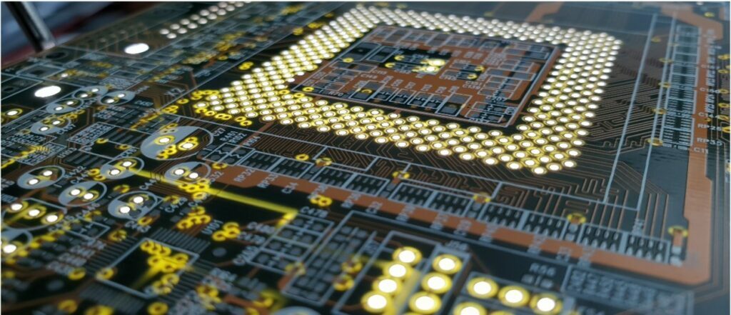
PCBs can be single-sided (one copper layer), double-sided (two copper layers on both sides of one substrate layer), or multilayer (outer and inner layers of copper, alternating with layers of substrate).
Multilayer PCBs allow for much higher component density because circuits on the inner layers would otherwise take up surface space between components. However, Multilayer PCBs make the repair, analysis, and field modification of circuits much more difficult and usually impractical.
Multilayer PCBs allow for much higher component density because circuits on the inner layers would otherwise take up surface space between components. However, Multilayer PCBs make the repair, analysis, and field modification of circuits much more difficult and usually impractical.
Line and space: 0.075mm / 0.075mm. Advanced 0,06mm / 0,06mm.
Layer count: Up to 26 layers. Advanced 42 layers
PCB material: FR4 raw material with high TG, low CTE, halogen-free, Hi-Speed and low loss specifications
Surface finish: OSP, HASL-LF ENIG.
Layer count: Up to 26 layers. Advanced 42 layers
PCB material: FR4 raw material with high TG, low CTE, halogen-free, Hi-Speed and low loss specifications
Surface finish: OSP, HASL-LF ENIG.
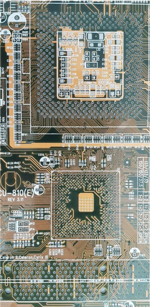
The Multilayer PCB is mainly used in professional electronic equipment, such as computers and military equipment. The Multilayer PCB is also very useful in high-speed circuits.
The Multilayer PCB can provide more space for the conductor pattern and power on the inner layers. The technology can be a solution for shielding trouble, impedance, and high-speed signal application.
The Multilayer PCB can provide more space for the conductor pattern and power on the inner layers. The technology can be a solution for shielding trouble, impedance, and high-speed signal application.
PCBs can be single-sided (one copper layer), double-sided (two copper layers on both sides of one substrate layer), or multilayer (outer and inner layers of copper, alternating with layers of substrate).
Multilayer PCBs allow for much higher component density because circuits on the inner layers would otherwise take up surface space between components. However, Multilayer PCBs make the repair, analysis, and field modification of circuits much more difficult and usually impractical.
Multilayer PCBs allow for much higher component density because circuits on the inner layers would otherwise take up surface space between components. However, Multilayer PCBs make the repair, analysis, and field modification of circuits much more difficult and usually impractical.
Line and space: 0.075mm / 0.075mm. Advanced 0,06mm / 0,06mm.
Layer count: Up to 26 layers. Advanced 42 layers
PCB material: FR4 raw material with high TG, low CTE, halogen-free, Hi-Speed and low loss specifications
Surface finish: OSP, HASL-LF ENIG.
Layer count: Up to 26 layers. Advanced 42 layers
PCB material: FR4 raw material with high TG, low CTE, halogen-free, Hi-Speed and low loss specifications
Surface finish: OSP, HASL-LF ENIG.
The Multilayer PCB is mainly used in professional electronic equipment, such as computers and military equipment. The Multilayer PCB is also very useful in high-speed circuits.
The Multilayer PCB can provide more space for the conductor pattern and power on the inner layers. The technology can be a solution for shielding trouble, impedance, and high-speed signal application.
The Multilayer PCB can provide more space for the conductor pattern and power on the inner layers. The technology can be a solution for shielding trouble, impedance, and high-speed signal application.
Industries
Industries
Telecom
Our desire to stay connected, always and everywhere, is the backbone of ICPRUS’s engineering know-how and one-stop solutions.
Consumer &
Multimedia
Multimedia
The Industrial Automation sector benefits from ICPRUS’s intimate understanding of the complexity of automation and robotics.
Industry
The Industrial Automation sector benefits from ICPRUS’s intimate understanding of the complexity of automation and robotics.
Automotive
Top Automotive brands choose ICPRUS to match and exceed the high quality and logistics demands of their industry.
TECHNICAL DATA
TECHNICAL DATA
Do you have any questions? Contact us!