Product Benefits
The Back-panel PCB serves as a backbone for the electronic system, providing a single point of connection for various electronic modules, daughterboards, and other PCBs. It typically contains many high-speed traces, connectors, and power distribution planes that allow for fast and efficient communication between the active sub-boards. The majority of Back-panel PCBs doesn´t contain any active components.
Ease of assembly
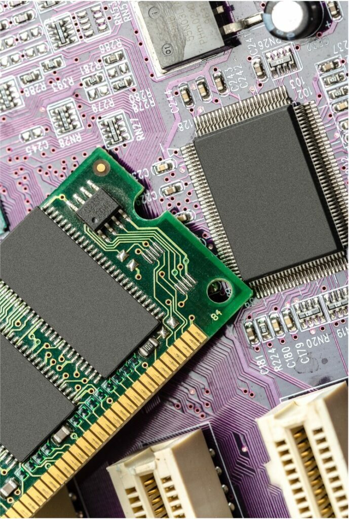
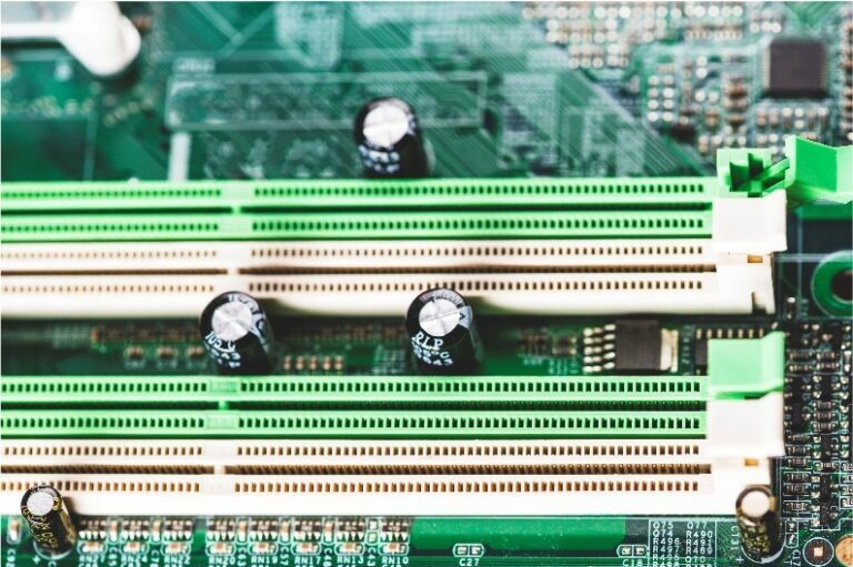
The primarily used components on Back-panels are the connectors used to interconnect the sub-boards. These can be Press-fitted, STM mounted or THT mounted.
Reliability
Back-panel technology provides superior reliability and high-speed connectivity compared with any other interconnection module solutions.
Wide range of materials
The base material of the back-panel must support high-speed impedance-controlled signal interconnection between various active sub-boards. Most back-panels are built from dedicated high-speed materials with low loss tangent(DF) and the epsilon relative(DK).
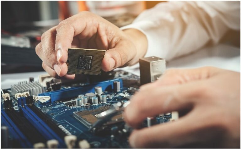
A back-panel PCB is often compared to a personal computer’s motherboard since both contain connections (slots) for sub-boards and allows for communication between all connected boards. The main difference is that the Motherboard used in computer systems contains active component and processors and connections (slots) for expansions boards, where the Back-panel often only contain connections (slots) to interconnect several active boards in larger Server systems.
Line and space: Back panel PCBs often require impedance-controlled traces which typically mean smaller trace and spacing widths with sizes as small as 0.0025, 0.003 or 0.004 inches (62, 75, 100 microns). Most manufacturers use laser direct imaging (LDI) and vacuum Develop-Etch-Strip (DES) lines to etch the fine patterns.
Vias: Vias are mainly mechanical drilled with min. size approximately 0,3mm. Low possible on request.
Layer count: up to 60 layers
PCB material: We normally recommend using mid or high Tg. material for Back-panel PCBs. Many applications with controlled trace impedances, require special high-speed materials with low signal loss dissipation factor (Df) & low epsilon relative, dielectric constant (εr Dk)
Surface finish: The Back-panel surface treatment depends upon the connector assembly method: Press-fit requires HASL, LF HASL or Immersion Sn. THT and SMT technology requires HASL, LF HASL, OSP, ENIG, Immersion Sn or Immersion Ag.
There are two types of back-panel systems: active and passive. Active back-panels contain the slots as well as the necessary circuitry to manage and control all the communication between the slots. In contrast, passive back panels contain almost no computing circuitry.
Back-panels often have a considerable size to support and interconnection of several sub-boards in a rack-system. The extreme number of wires required to interconnect the sub-boards often results in high amount of layers. This makes Back-panels thicker and more Rigid than most PCB. This is a benefit since the PCB needs to be stiff enough to support the insertion force plugging the sub-boards into the back-panel connectors. Rigid-Multilayers are the most common technology used to develop back panels, but Flex-Rigid can also be developed in the case of special cabinet solution.
Back-panels are the backbone for any larger computing or server system. It offers a firm and robust mechanical platform allow low-ohm high-speed interconnection between all the sub-boards the complex electronic system.
Aratek biometric solutions
streamlines identity
management for millions
streamlines identity
management for millions
Industries
Aratek biometric solutions
streamlines identity
management for millions
streamlines identity
management for millions
Industries
Power / Energy
Our electrifying world thrives from ICPRUS’s engineering expertise to safely allow for the high voltages and currents to carry our energy.
Metering
With ultra-modern laboratories and equipment, ICPRUS guarantees long product life and high quality.
Automotive
Top Automotive brands choose ICPRUS to match and exceed the high quality and logistics demands of their industry.
Medical
An ever-increasing amount of companies in the medical industry rely on the Precision from ICPRUS.
Industry
The Industrial Automation sector benefits from ICPRUS’s intimate understanding of the complexity of automation and robotics.
Consumer &
Multimedia
Multimedia
The Industrial Automation sector benefits from ICPRUS’s intimate understanding of the complexity of automation and robotics.
Aratek biometric solutions
streamlines identity
management for millions
streamlines identity
management for millions
Technical Data
Aratek biometric solutions
streamlines identity
management for millions
streamlines identity
management for millions
Technical Data
Do you have any questions? Contact us!